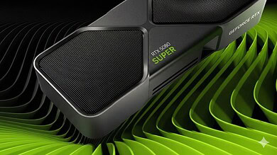
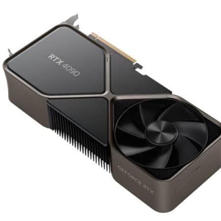
NVIDIA GeForce RTX 4090 “Ada Lovelace” Graphics Card Launched
16384 Cores, 24 GB GDDR6X, 4X Faster Than RTX 3090 at $1599 US
NVIDIA GeForce RTX 4090 is here as the next-gen BFGPU, offering earth-shattering performance that takes gaming to the next level. The GeForce RTX 4090 isn’t just a GPU, it’s the flagship green team offering, and offers four times the performance increases over its predecessor.
NVIDIA Takes Gaming To The Next Level… not.
NVIDIA’s GeForce RTX 4090 has been long-awaited and now it’s finally here. Nvidia keeps its usual editorial stance : The graphics card is designed for enthusiasts and gamers who want the best visual fidelity
The truth is much more blurry. This card and its announced MSRP ($1,599) firmly keeps it out of 99% of gamers out there. As NVIDIA was designing and pushing the RTX 4090 into production line, crypto miners where a primary focus and mammoth size memory shows it (24 GB DDR6X).
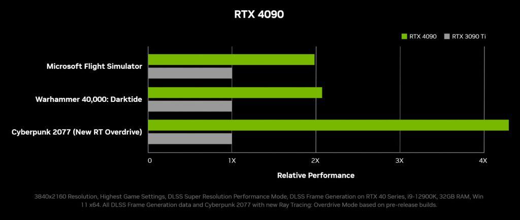
As far as gaming goes, sure it’ll do great. We got a 35% performance increase when compared to its predecessor (GeForce RTX 3090Ti ) and a whole 4x faster with DLSS and 2x faster in native resolution for faster fps and Ray Tracing.
But he question remain, what gamer on earth can afford this. If MSRP is at $1,600 it means partner cards going at no less than 2 full grand.
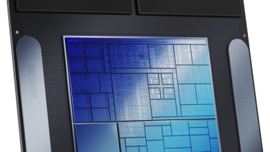
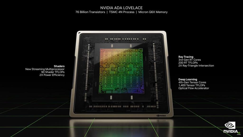
NVIDIA’s AD102 ‘Ada Lovelace’ GPU – The Next-Gen Powerhouse
Now that’s said, let’s take a look at what is in the AD102 GPU itself:
The GPU measures 608,4mm2 and will utilize the TSMC 4N process node which is an optimized version of TSMC’s 5nm (N5) node designed for the green team. The GPU features an insane 76.3 Billion transistors.
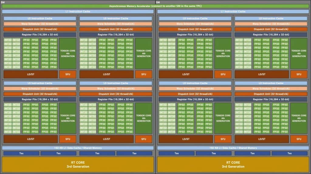
The NVIDIA Ada Lovelace AD103 GPU is expected to feature up to 7 GPC (Graphics Processing Clusters). This is the same GPC count as the Ampere GA102 GPU and one additional GPC over the GA103 GPU. Each GPU will consist of 6 TPCs and 2 SMs which is the same configuration as the existing chip. Each SM (Streaming Multiprocessor) will house four sub-cores which is also the same as the GA102 GPU. What’s changed is the FP32 & the INT32 core configuration. Each sub-core will include 128 FP32 units but combined FP32+INT32 units will go up to 192. This is because the FP32 units don’t share the same sub-core as the IN32 units. The 128 FP32 cores are separate from the 64 INT32 cores.
So in total, each sub-core will consist of 32 FP32 plus 16 INT32 units for a total of 48 units. Each SM will have a total of 128 FP32 units plus 64 INT32 units for a total of 192 units. And since there are a total of 84 SM units (12 per GPC), we are looking at 12,288 FP32 Units and 6,144 INT32 units for a total of 18,432 cores. Each SM will also include two Wrap Schedules (32 thread/CLK) for 64 wraps per SM. This is a 50% increase on the cores (FP32+INT32) and a 33% increase in Wraps/Threads vs the GA102 GPU.
NVIDIA AD102 ‘Ada Lovelace’ Gaming GPU ‘SM’ Block Diagram (Image Credits: Kopite7kimi):
| GPU NAME | AD102 | GA102 | TU102 | GA100 | GH100 |
|---|---|---|---|---|---|
| GPC | 12 (Per GPU) | 1.7x | 2x | 1.5x | 1.5x |
| TPC | 6 (Per GPC) | Same | Same | 0.75x | 0.67x |
| SM | 2 (Per TPC) | Same | Same | Same | Same |
| Sub-Core | 4 (Per SM) | Same | Same | Same | Same |
| FP32 | 128 (Per SM) | Same | 2x | 2x | Same |
| FP32+INT32 | 192 (Per SM) | 1.5x | 1.5x | 1.5x | Same |
| Warps | 64 (Per SM) | 1.33x | 2x | Same | Same |
| Threads | 2048 (Per SM) | 1.33x | 2x | Same | Same |
| L1 Cache | 192 KB (Per SM) | 1.5x | 2x | Same | 0.75x |
| L2 Cache | 96 MB (Per GPU) | 16x | 16x | 2.4x | 1.6x |
| ROPs | 32 (Per GPC) | 2x | 2x | 2x | 2x |
Moving over to the cache, this is another segment where NVIDIA has given a big boost over the existing Ampere GPUs. The Ada Lovelace GPUs will pack 192 KB of L1 cache per SM, an increase of 50% over Ampere. That’s a total of 4.5 MB of L1 cache on the top AD102 GPU. The L2 cache will be increased to 96 MB as mentioned in the leaks. This is a 16x increase over the Ampere GPU that hosts just 6 MB of L2 cache. The cache will be shared across the GPU.
Finally, we have the ROPs which are also increased to 32 per GPC, an increase of 2x over Ampere. You are looking at up to 384 ROPs on the next-gen flagship versus just 112 on the fastest Ampere GPU, the RTX 3090 Ti. There are also going to be the latest 4th Generation Tensor and 3rd Generation RT (Raytracing) cores infused on the Ada Lovelace GPUs which will help boost DLSS & Raytracing performance to the next level. Overall, the Ada Lovelace AD102 GPU will offer:
- 2x GPCs (Versus Ampere)
- 50% More Cores (Versus Ampere)
- 50% More L1 Cache (Versus Ampere)
- 16x More L2 Cache (Versus Ampere)
- Double The ROPs (Versus Ampere)
- 4th Gen Tensor & 3rd Gen RT Cores
NVIDIA GeForce RTX 4090 ‘Official’ Specifications
The NVIDIA GeForce RTX 4090 will use 128 SMs of the 144 SMs for a total of 16,384 CUDA cores. The GPU will come packed with 96 MB of L2 cache and a total of 384 ROPs which is simply insane but considering that the RTX 4090 is a cut-down design, it may feature slightly lower L2 and ROP counts. The clock speeds are not confirmed yet but considering that the TSMC 4N process is being used. The clock speeds are rated at up to 2.6 GHz and NVIDIA is claiming over 3 GHz speeds with overclocking.
As for memory specs, the GeForce RTX 4090 will feature 24 GB GDDR6X capacities that will be clocked at 21 Gbps speeds across a 384-bit bus interface. This will provide up to 1 TB/s of bandwidth. This is the same bandwidth as the existing RTX 3090 Ti graphics card and as far as the power consumption is concerned, the TBP is rated at 450W. The card will be powered by a single 16-pin connector which delivers up to 600W of power. Custom models will be offering higher TBP targets.
NVIDIA GeForce RTX 4090 Graphics Cards Performance
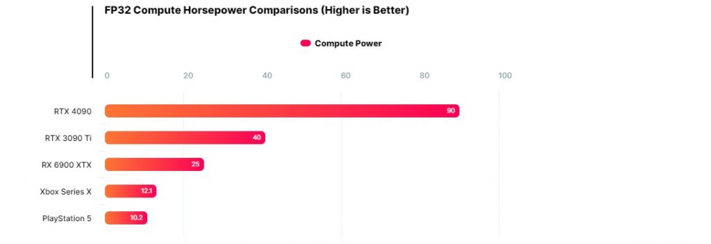
As for the performance of these monster GPUs, NVIDIA shared the computational and gaming performance figures and it looks like the GeForce RTX 4090 will be the first gaming card to hit the 100 TFLOPs compute horsepower limit.
Just for comparison’s sake:
- NVIDIA GeForce RTX 4090: 90 TFLOPs (FP32) (Assuming 2.8 GHz clock)
- NVIDIA GeForce RTX 3090 Ti: 40 TFLOPs (FP32) (1.86 GHz Boost clock)
- NVIDIA GeForce RTX 3090: 36 TFLOPs (FP32) (1.69 GHz Boost clock)
Based on a theoretical clock speed of 2.8 GHz, you get up to 103 TFLOPs of compute performance and the rumors are suggesting even higher boost clocks. Now, these are definitely sounding like peak clocks, similar to AMD’s peak frequencies which are higher than the average ‘Game’ clock. A 100+ TFLOPs compute performance means more than double the horsepower versus the 3090 Ti flagship. But one should keep in mind that compute performance doesn’t necessarily indicate the overall gaming performance but despite that, it will be a huge upgrade for gaming PCs and an 8.5x increase over the current fastest console, the Xbox Series X.
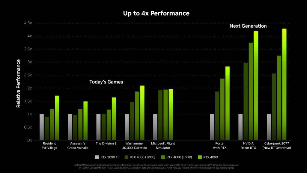
This will be a 2x compute performance uplift and a 2x gain in gaming performance as NVIDIA has demonstrated for each graphics card versus its predecessor and this is without even factoring in the RT and Tensor core performance which are expected to get major lifts too in their respective department. A 2-4x gain over the RTX 3090 & RTX 3090 Ti would be very disruptive.
Gamers (sic) should expect 4K gaming to be buttery smooth on these graphics cards and with DLSS, we might even see playable 60 FPS at 8K resolution which is something that NVIDIA has been trying to achieve with its RTX 3090 series BFGPUs for a while now.
NVIDIA GeForce RTX 4090 Graphics Cards Price & Availability
Now coming to the prices, the NVIDIA GeForce RTX 3090 Ti & RTX 3090 graphics cards are without a doubt the most expensive single-chip GPUs to date. The NVIDIA GeForce RTX 4090 is going to come at a price of $1599 US for the Founders Edition, and probably much more on the real-world market, and variant and will be available on the 12th of October.
NVIDIA GeForce RTX 40 Series Preliminary Specs:
| GRAPHICS CARD NAME | NVIDIA GEFORCE RTX 4090 | NVIDIA GEFORCE RTX 4080 16G | NVIDIA GEFORCE RTX 4080 12G | NVIDIA GEFORCE RTX 3090 TI | NVIDIA GEFORCE RTX 3080 |
|---|---|---|---|---|---|
| GPU Name | Ada Lovelace AD102-300? | Ada Lovelace AD103-300? | Ada Lovelace AD104-400? | Ampere GA102-225 | Ampere GA102-200 |
| Process Node | TSMC 4N | TSMC 4N | TSMC 4N | Samsung 8nm | Samsung 8nm |
| Die Size | 608mm2 | ~450mm2 | ~450mm2 | 628.4mm2 | 628.4mm2 |
| Transistors | 76 Billion | TBD | TBD | 28 Billion | 28 Billion |
| CUDA Cores | 16384 | 9728 | 7680 | 10240 | 8704 |
| TMUs / ROPs | TBD | TBD | TBD | 320 / 112 | 272 / 96 |
| Tensor / RT Cores | TBD / TBD | TBD / TBD | TBD / TBD | 320 / 80 | 272 / 68 |
| Base Clock | 2230 MHz | 2210 MHz | 2310 MHz | 1365 MHz | 1440 MHz |
| Boost Clock | 2520 MHz | 2510 MHz | 2610 MHz | 1665 MHz | 1710 MHz |
| FP32 Compute | 90 TFLOPs | 49 TFLOPs | 40 TFLOPs | 34 TFLOPs | 30 TFLOPs |
| RT TFLOPs | TBD | TBD | TBD | 67 TFLOPs | 58 TFLOPs |
| Tensor-TOPs | TBD | TBD | TBD | 273 TOPs | 238 TOPs |
| Memory Capacity | 24 GB GDDR6X | 16 GB GDDR6X | 12 GB GDDR6X | 12 GB GDDR6X | 10 GB GDDR6X |
| Memory Bus | 384-bit | 256-bit | 192-bit | 384-bit | 320-bit |
| Memory Speed | 21.0 Gbps | 23.0 Gbps | 21.0 Gbps | 19 Gbps | 19 Gbps |
| Bandwidth | 1008 GB/s | 736 GB/s | 504 GB/s | 912 Gbps | 760 Gbps |
| TBP | 450W | 320W | 285W | 350W | 320W |
| Price (MSRP / FE) | $1599 US | $1199 US | $899 US | $1199 | $699 US |
| Launch (Availability) | October 2022 | November 2022 | November 2022 | 3rd June 2021 | 17th September 2020 |