RELEASE DATE
Source: WCCFTECH
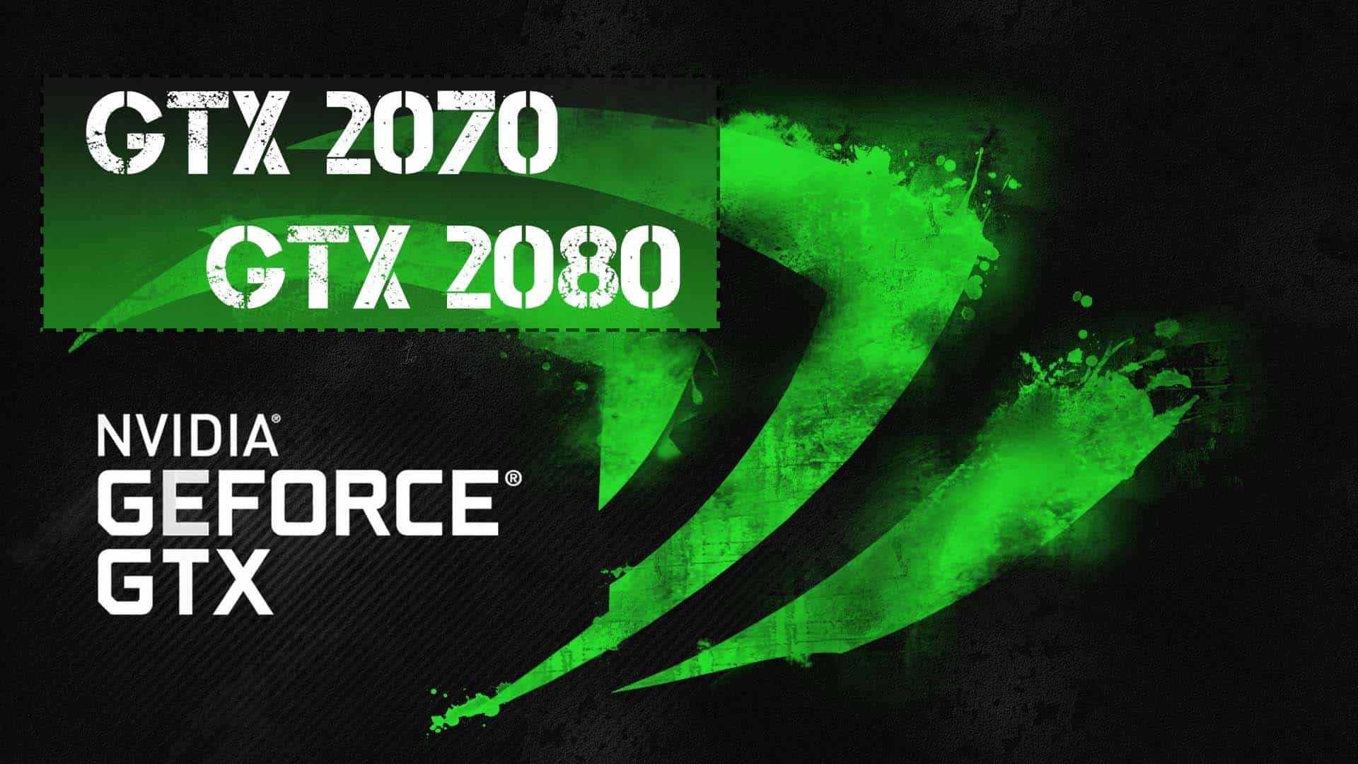
Finally, the wait is almost over. Without saying it, Nvidia let the world know that their new and long-awaited GPU series, the GTX 2070 and the GTX 2080 video-cards, will be launch at Gamescom on the 20th of August.
PRICING
These are the expected MSRPs that AIB and vendors have been informed of by NVIDIA:
- The 120W NVIDIA next-gen GPU (GeForce GTX 2065?) will be priced around $499 MSRP.
- The 150W NVIDIA next-gen GPU (GeForce GTX 2070?) will be priced around $599 MSRP.
- The 180W NVIDIA next-gen GPU (GeForce GTX 2080?) will be priced around $699-749 MSRP.
At the same time,
- The GeForce GTX 1080 Ti MSRP will drop in price by $100.
- The GeForce GTX 1080 MSRP will drop in price by $50.
These are unconfirmed prices, but I believe that based on what is going around online, it should not be too far from what will be announced in a couple of weeks.
SPECS
Source: WCCFTECH
Manli Technologies, a vendor for NVIDIA GeForce GPUs has just registered an ECC certificate with the name GeForce GTX 2070 and GeForce GTX 2080 included in the mix. The GPU chips also contain GA104 and GA104-400 – both of which are Ampere based.
Source : VideoCardz
| Model | GPU | Clocks | Memory | |
|---|---|---|---|---|
 | NVIDIA GeForce GTX 2070 | GA104 | / 1750 MHz | 8 GB GDDR6 |
 | NVIDIA GeForce GTX 2080 | GA104-400 | / 1750 MHz | 8 GB GDDR6 |
GEFORCE GTX 2070
| Overview | |
| Manufacturer | NVIDIA |
| Original Series | GeForce 20 |
| Release Date | 20th of August 2018 (Q2 2018) |
| Graphics Processing Unit | |
| GPU Model | GA104 |
| Architecture | Ampere |
| Fabrication Process | 12 nm FinFET |
| Clocks | |
| Base Clock | TBD |
| Boost Clock | TBD |
| Memory Clock | 1750 MHz |
| Effective Memory Clock | 14000 Mbps |
| Memory Configuration | |
| Memory Size | 8192 MB |
| Memory Type | GDDR6 |
| Memory Bus Width | 256-bit |
| Memory Bandwidth | 448 GB/s |
GEFORCE GTX 2080
| Overview | |
| Manufacturer | NVIDIA |
| Original Series | GeForce 20 |
| Release Date | 20th of August 2018 (Q2 2018) |
| Graphics Processing Unit | |
| GPU Model | GA104-400 (GA104) |
| Architecture | Ampere |
| Fabrication Process | 12 nm FinFET |
| Clocks | |
| Base Clock | TBD |
| Boost Clock | TBD |
| Memory Clock | 1750 MHz |
| Effective Memory Clock | 14000 Mbps |
| Memory Configuration | |
| Memory Size | 8192 MB |
| Memory Type | GDDR6 |
| Memory Bus Width | 256-bit |
| Memory Bandwidth | 448 GB/s |